[Verilog] Gate-Level Modeling
AND/OR Gates

these gates are instantiated to build logic circuits
truth tables assuming two inputs

BUF/NOT Gates
BUF/NOT gates have one scalar input, several scalar output

- buf : 입력을 그대로 출력해주는 장치
노이즈가 생겼을 때 버퍼를 통과하면 노이즈가 사라진다. 주목할 점은 z를 넣으면 x가 output으로 나온다. - not : 입력을 반대로 출력해주는 장치
output이 2개 이상 있을 수 있다.
not n1 (OUT1, OUT2, IN);
Gates with an additional control signal on BUF/NOT gates are also available.
→ bufif1, bufif0, notif1, notif0
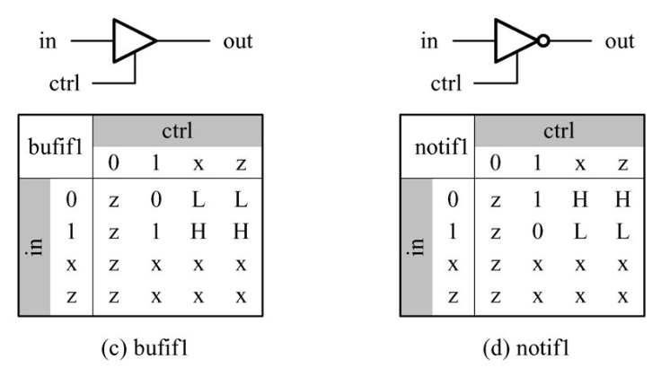
* H : a value 1 or z
* L : a value 0 or z
- bufif1
일반 버퍼에 ctrl이 붙어있는 형태.
ctrl이 1일 때만 버퍼의 역할이 실행된다. 즉, 0일 때에는 선이 연결되지 않은 상태로 간주한다.
- bufif0
ctrl이 0일 때만 버퍼의 역할이 실행됨. - notif0, notif1
notif1 : ctrl 이 1일 때 not이 작동함
notif0 : ctrl 이 0일 때 not이 작동함
Array of Instances
verilog HDL allows an array of primitive instances to be defined
wire [7:0] OUT, IN1, IN2;

nand n_gate[7:0] (OUT, IN1, IN2);

nand n_gate0(OUT[0], IN1[0], IN2[0]);
nand n_gate1(OUT[1], IN1[1], IN2[1]);
nand n_gate2(OUT[2], IN1[2], IN2[2]);
nand n_gate3(OUT[3], IN1[3], IN2[3]);
...
이런 식으로 묶어서 관리하면 더 편리하게 사용할 수 있다.
Gate-Level Multiplexer
gate-level의 multiplexer를 제작해볼 것이다.

multiplexer의 내부 구조는 위와 같다.

- mux module
module mux4_to_1 (out, i0, i1, i2, i3, s1, s0);

output out;
input i0, i1, i2, i3;
input s1, s0;

wire s1n, s0n;
wire y0, y1, y2, y3;

not(s1n, s1);
not(s0n, s0);

and(y0, i0, s1n, s0n);
and(y1, i1, s1n, s0);
and(y2, i2, s1, s0n);
and(y3, i3, s1, s0);

or(out, y0, y1, y2, y3);

endmodule
회로 그대로 연결했다고 생각하면 이해가 쉽다.
- stimulus module
module stimulus

reg IN0, IN1, IN2, IN3;
reg S1, S0;

wire OUTPUT;

mux4_to_1 mymux(OUTPUT, IN0, IN1, IN2, IN3, S1, S0);

initial
begin

// simulate 진행하기

end
endmodule
4-bit Ripple Carry Full Adder
1. Designing a 1-bit full adder
sum = a (xor) b (xor) cin
cout (a * b) (xor) cin * (a (xor) b)

module fulladd(sum, c_out, a, b, c, c_in);

output sum, c_out;
input a, b, c, c_in;

wire s1, c1, c2;

xor(s1, a, b);
and(c1, a, b);

xor(sum, s1, c_in);
and(c2, s1, c_in);

xor(c_out, c2, c1);

endmodule
2. 4-bit ripple carry full adder
ripple carry full adder는 full adder를 4개 결합한 형태이다.
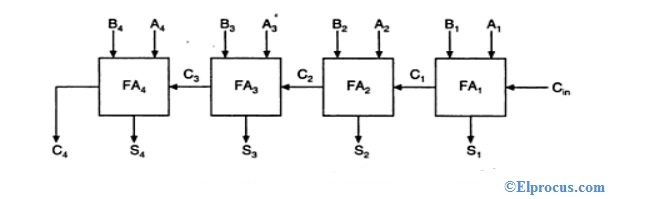
module fulladd4(sum, c_out, a, b, c_in);

output [3:0] sum;
output c_out;
input[3:0] a, b;
input c_in;

wire c1, c2, c3;

fulladd fa0(sum[0], c1, a[0], b[0], c_in);
fulladd fa1(sum[1], c1, a[1], b[1], c1);
fulladd fa2(sum[2], c1, a[2], b[2], c2);
fulladd fa3(sum[3], c1, a[3], b[3], c3);

endmodule
Rise, Fall, and Turn-off Delays
모든 전기신호는 회로를 통과하는 과정에서 delay가 발생할 수 밖에 없다.
- Rise delay0, x, z → 1
- Associated with a gate output transition to a 1 from another value
- Fall delay1, x, z → 0
- Associated with a gate output transition to a 0 from another value
- turn-off delay0, 1, x → z
- Associated with a gate output transition to the high impedance value ( z )
- 사용법 딜레이가 하나만 설정되어있다면 모든 transition에 사용된다.딜레이가 없으면 기본 값은 0이다.
// #(rise_delay, fall_delay, turn-off delay) add #(5) al (out, i1, i2); //delay of 5 for all transition add #(4, 6) a2 (out, i1, i2); // rise delay = 4, fall delay = 6, turnoff = 4 bufif0 #(3,4,5) b1 (out, in, control); //rise = 3, in = 4, control = 5- 만약 두개라면 rise, fall delay가 설정되고 turn-off 는 더 작은 값으로 설정된다.
- #(delay time) 으로 사용한다.
Min/Typ/Max Values
additional level of control for each type of delay
→ delay의 각 타입에 min/typ/max value를 각각 설정해줄 수 있다.
default : typical delay
These values can be chosen at Verilog run time.
add #(2:3:4, 3:4:5, 4:5:6) a3(out, i1, i2);
실행시킬 때 delay 설정하는 방법
> verilog test.v +maxdelays
// maxdelays 대신 mindelays, typdelays로 변경 가능
Delay Example
- 구현 모듈 회로
and : delay 5 , or : delay 4

위 모듈이 작동하는 과정을 timing diagram으로 표현하면 아래와 같다.

'Computer Science > Verilog & HW' 카테고리의 다른 글
| [Verilog] Dataflow Modeling (1) | 2023.10.09 |
|---|---|
| [Verilog] Modules and Ports (0) | 2023.05.19 |
| [Verilog] Basic Concept (0) | 2023.02.01 |
| [Verilog] Hierarchical Modeling Concepts (0) | 2023.02.01 |